Views: 0 Author: Site Editor Publish Time: 2026-05-19 Origin: Site


Consumer electronics continue shrinking in form factor at an aggressive pace. Devices like wearables, extended reality (XR) headsets, and 5G smartphones pack complex components closer together than ever before. This extreme density exponentially increases the risks of cross-talk, thermal failure, and environmental damage. Engineering teams face tough choices early in the design cycle.
You can no longer treat component shielding and sealing as a late-stage afterthought. It requires balancing strict ingress protection (IP) ratings and acoustic fidelity with high-volume manufacturing realities. Choosing the wrong materials often leads to costly product recalls, compromised signal integrity, and manufacturing delays.
This guide breaks down the critical evaluation criteria for device shielding, sealing, and thermal management components. We will examine implementation risks, supply chain scalability, and verifiable performance metrics. You will learn how to build resilient, high-performance devices without creating assembly line bottlenecks.
Interference Management: Effective EMI/RFI shielding requires analyzing Z-axis conductivity and passive intermodulation (PIM) reduction, often replacing bulky metal shields with lightweight device protection tape.
Moisture vs. Breathability: Achieving high IP ratings without sacrificing acoustic performance or thermal dissipation requires a hybrid approach of sealing components and micro-venting for pressure equalization.
Coating Trade-offs: Selecting PCB waterproofing requires weighing the upfront capital and rework impossibility of Parylene against the masking-labor costs of traditional conformal coatings and the agile deployment of modern nano-coatings.
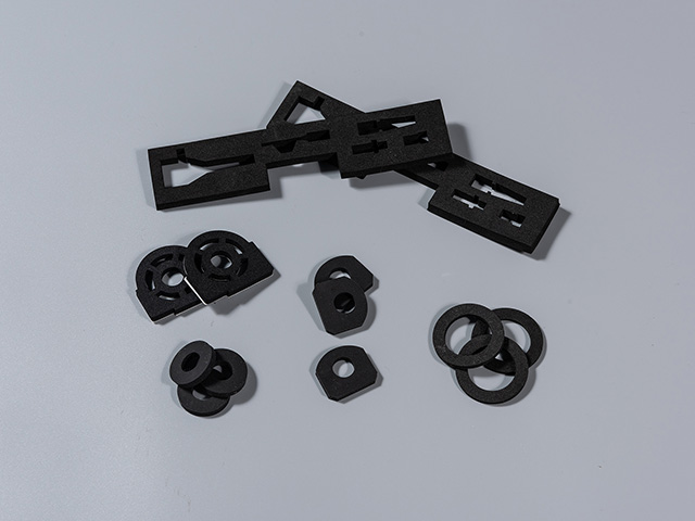
Assembly Realities: The true cost of any insulation material is dictated by its application method—die-cut fabrication, push-through connectivity, and room-temperature curing drastically reduce manufacturing bottlenecks.
Devices rarely face a single point of stress in real-world scenarios. A modern 5G smartphone battles extreme processor heat while handling millimeter-wave interference. It must simultaneously fight off external moisture ingress from rain or sweat. We cannot view these hazards in isolation. Protecting internal architecture requires a comprehensive approach.
A viable protection strategy demands verifiable compliance. Materials must pass rigorous standards like UL 94V-0 for flammability. They must achieve specific IPX ratings for water resistance. However, you must hit these benchmarks without adding unacceptable weight or volume to the final product. Every extra millimeter matters in consumer hardware.
We must apply system-level thinking to navigate these overlapping constraints. Designing robust device protection means categorizing engineering countermeasures into four distinct disciplines:
Thermal and Electrical Insulation: Stopping stray currents and routing heat away from sensitive processors.
EMI/RFI Management: Blocking electromagnetic noise from overlapping frequencies.
Environmental Sealing: Creating physical barriers against dust, chemicals, and liquids.
Acoustic Damping: Reducing internal vibration and mechanical noise without muffling audio output.
Engineers categorize thermal and electrical solutions into two primary buckets. First, we use dielectric barriers to block stray electrical currents. These include polyimide films, PET tapes, and flame-retardant polypropylene. They prevent arcing and stop catastrophic short circuits across tight board layouts. Second, we deploy thermal interface materials (TIMs). Thermally conductive fiberglass tapes and silicone pads act as heat bridges. They aggressively route thermal loads away from CPUs and MOSFETs toward outer heat sinks.
When selecting electronic insulation, you must evaluate multiple performance dimensions. Dielectric strength versus thickness remains paramount. We assess the breakdown voltage per mil of material. High dielectric strength allows you to use thinner films, keeping device profiles ultra-sleek. You must also verify absolute thermal limits. Check continuous operating temperature ranges. Ensure the materials possess self-extinguishing properties matching strict aviation-grade or consumer safety standards.
Implementation carries distinct risks. Materials often degrade under continuous thermal cycling. Device components expand and contract as they heat and cool. Ensure your chosen insulation material resists long-term adhesive breakdown. It should never suffer from chemical outgassing over the product lifecycle, as outgassing can fog camera lenses or foul sensitive sensors.
Always match the TIM hardness to your mechanical tolerance; softer pads fill micro-voids better.
Avoid over-compressing thermal pads, which can rupture internal fiberglass matrices.
Test dielectric films in high-humidity chambers, as moisture absorption severely lowers voltage breakdown thresholds.
Signal interference ruins user experiences. Tight spaces breed passive intermodulation (PIM). Extended reality (XR) headsets and 5G transceiver modules suffer heavily from frequency overlapping. Poorly shielded components degrade signal integrity, drop network connections, and cause erratic device behaviors.
Traditional manufacturing relied on stamped metal shield cans. They worked well for older hardware, but they remain bulky and heavy. Grounding them flexibly across curved or movable joints proves incredibly difficult. Modern engineering shifts heavily toward isotropic (XYZ-axis) and anisotropic (Z-axis only) conductive electronics tape.
Replacing metal cans yields immediate hardware benefits. You can use conductive fabric or copper foil device protection tape to save vital Z-height inside the chassis. This approach drops weight while maintaining shielding effectiveness at or above 60 dB. Applying smart grounding tapes to display ribbons and camera modules prevents adjacent circuit shorts. These tapes maintain extremely low contact resistance, typically keeping it below 0.1 ohms.
We must remain transparent about physical assumptions. Conductive tapes provide highly effective flexible grounding, but they rely entirely on process control. Their performance depends heavily on the precision of the die-cut edges. Consistent application pressure during assembly remains critical to activate the conductive particles embedded within the adhesive layer.
Summary Chart: Traditional Shields vs. Conductive Tapes | |||
Shielding Method | Weight / Volume Impact | Grounding Flexibility | Implementation Challenge |
|---|---|---|---|
Stamped Metal Cans | High weight, consumes large Z-height | Rigid, fixed to specific solder points | Requires dedicated board space and wave soldering |
Isotropic Tape (XYZ) | Ultra-lightweight, minimal thickness | Excellent for complex geometries | Requires precise pressure to activate conductivity |
Anisotropic Tape (Z-axis) | Ultra-lightweight, isolates XY axes | Perfect for tight, adjacent circuitry | Dependent on highly accurate die-cut fabrication |
Consumers often misunderstand waterproofing. We must separate the engineering reality of "water-resistant" from "waterproof." Water-resistant materials simply delay liquid ingress. Waterproofing implies a completely impermeable barrier. Designing consumer hardware requires navigating this spectrum carefully.
We deploy two distinct categories of environmental solutions. First, we use physical barriers. These include custom-molded silicone gaskets, non-blooming TPE overmolds, and dielectric greases applied to ports. Second, we integrate pressure equalization components. Acoustic and protective vents utilize expanded polytetrafluoroethylene (ePTFE) membranes to manage airflow.
Engineers inevitably face the Sealing Paradox. Completely sealing a device traps processor heat inside the shell. Furthermore, altitude shifts and temperature swings create massive internal pressure differentials. Unmitigated pressure blows out delicate silicone seals. It distorts internal acoustic components like speakers and microphones, ruining audio fidelity.
Your decision logic should pair robust physical seals with breathable micro-vents. You use heavy gaskets for structural gaps. You install ePTFE vents to balance internal pressure. These micro-porous membranes allow air and sound waves to pass freely while blocking liquid droplets and dust particles.
Relying on standard double-sided tape instead of dedicated closed-cell foam gaskets for liquid barriers.
Failing to account for thermal expansion, causing rigid structural seals to crack over time.
Believing "100% waterproof" marketing claims for permeable textiles; always evaluate materials strictly against standardized IP67 or IPX8 test protocols.
Unmitigated moisture destroys printed circuit boards. Humid environments lead to ionic corrosion and electrical waveform distortion. Moisture accelerates the growth of conductive "tin whiskers" between solder joints. These microscopic metal filaments eventually bridge gaps, causing catastrophic short circuits.
Selecting the right PCB coating demands a clear versus framework. Let us compare the four dominant industry approaches:
Comparative Analysis of PCB Coating Methods | |||
Coating Type | Protection Level | Manufacturing Drawbacks | Reworkability |
|---|---|---|---|
Potting (Resin Encasement) | Maximum shock and extreme high-voltage arc resistance. | Adds massive weight and bulk; slow curing process. | Impossible. Components cannot be salvaged. |
Traditional Conformal Coating | Good moisture resistance (semi-permeable). | Requires intensive manual masking of connectors; long thermal cure times. | Moderate. Requires harsh chemical stripping. |
Parylene (Vacuum Deposition) | Flawless edge coverage; absolute pinpoint thickness. | Requires high capital expenditure for vacuum chambers; severe bottlenecks. | Extremely difficult. Often destroys the board. |
Nano-Coating (Fluoropolymers) | IPX4 to IPX8 protection; outstanding moisture barrier. | May require UV tracers for visual quality inspection. | Excellent. Features push-through connectivity. |
Implementation considerations directly dictate manufacturing success. Modern nano-coatings utilize transition metal complexes (TMC) and fluoropolymers. They offer immediate room-temperature curing. Most importantly, they enable "push-through connectivity." Testing probes and connector pins can physically pierce the nanometer-thick layer to establish electrical contact. This entirely eliminates the need for labor-intensive masking tape.
The true manufacturing burden of PCB protection lies in labor and cycle time. Solutions that eliminate masking steps and allow rapid component rework heavily reduce production bottlenecks. Shifting away from legacy conformal coatings directly improves overall manufacturing yields.
Identifying the right supply chain partner separates successful product launches from costly delays. You must evaluate suppliers based on rigid shortlisting logic. First, examine their volume and customization capabilities. Does the supplier offer rapid prototyping? High-tier partners provide three-day turnarounds for custom gasket molds. Suppliers relying solely on rigid, off-the-shelf SKUs rarely adapt well to innovative hardware geometries.
Next, scrutinize compliance and corporate governance. Verify whether the consumer electronics accessories meet global RoHS and REACH directives. Ask about environmental, social, and governance (ESG) options. Many modern suppliers provide bio-based or recycled-content elastomers. Utilizing these sustainable materials helps fulfill corporate carbon-neutral goals without sacrificing durability.
Finally, assess their fabrication capabilities. Look for supply chain partners offering total solution die-cutting. Elite fabricators can combine pressure-sensitive adhesives, thermal layers, and EMI shielding into a single deliverable part. Consolidating multiple layers into one component drastically reduces manual assembly steps.
Your immediate next action requires physical validation. Request sample rolls of tapes and membranes from your shortlisted suppliers. Test peel-strength values directly on your own substrate materials. Run these electronics accessories through thermal-cycling chambers within your specific manufacturing environment.
Selecting proper insulation and protection components dictates overall product lifespan and guarantees user safety.
Shift your engineering focus away from simply passing minimum IP or EMC compliance; prioritize optimizing manufacturing yields instead.
Embrace modern techniques like breathable ePTFE venting, masking-free nano-coatings, and multi-functional conductive tapes.
OEMs can build significantly more resilient devices without inflating labor and assembly timelines.
Your next step is to initiate physical prototyping and rigorous environmental stress testing using your shortlisted material formats.
A: Electrical insulation tape uses dielectric materials like PET or Polyimide to prevent current transfer and protect against short circuits. Conductive electronics tape uses metal foils or conductive adhesives to ground components and block EMI/RFI signals actively.
A: No. Traditional conformal coatings are semi-permeable. They are highly effective at preventing moisture damage and humidity-induced leakage, but they are not designed for continuous underwater submersion (IPX8) without additional physical enclosures or advanced nano-coatings.
A: Acoustic vents utilize micro-porous membranes, such as ePTFE. These materials allow air and sound waves to pass through freely, equalizing pressure and maintaining audio fidelity. Simultaneously, the microscopic pores remain too small for water droplets and dust particles to penetrate.
A: In 5G and XR devices with overlapping frequencies, poor grounding contacts or dissimilar metals can create PIM. This generates background noise that heavily degrades signal integrity. High-performance shielding tapes are formulated to maintain low, stable contact resistance to minimize this disruptive effect.


