Views: 0 Author: Site Editor Publish Time: 2026-05-18 Origin: Site


Consumer electronics constantly shrink in their Z-axis height. Yet, they house densely packed, multi-frequency components within these microscopic spaces. You will find Wi-Fi modules, Bluetooth transmitters, cellular radios, and high-speed processors crammed closely together. This physical proximity creates a severe operational problem. Unmanaged crosstalk and external electromagnetic noise run rampant across the circuit board. Left unchecked, these interferences lead to dropped wireless connections, sudden device failure, and regulatory compliance rejections.
Engineering teams must move beyond basic structural concepts to solve these complex interference issues. You need a clear, evidence-based framework to design robust hardware. This framework helps you evaluate and select the exact electrical conductive product required for your specific application. Our guide explores how to balance strict attenuation requirements, assembly scalability, and tight weight constraints. You will learn to navigate the physical realities of high-frequency interference and secure reliable electromagnetic compatibility for your next-generation devices.
Material matching depends on structural levels: PCB-level interference requires different solutions (e.g., metal cans or conductive tapes) than system-level plastic housing leaks (e.g., conductive coatings).
Secondary benefits drive ROI: Modern electronic shielding tape and conductive elastomers offer multi-functional value, including thermal management and galvanic corrosion prevention.
Physical design rules dictate performance: True EMI shielding effectiveness relies on strict mechanical tolerances, such as maintaining a 10%–30% gasket compression rate and keeping surface gaps below 1/20 of the target wavelength.
High-frequency realities: Above 900 MHz, the skin effect dominates; material thickness beyond 0.05 mm yields diminishing returns for standard metals, shifting the focus to application method and gap sealing.
Modern hardware packs immense processing power into incredibly tiny footprints. A standard flagship smartphone easily contains six or more close-proximity interference sources. Processors, OLED display drivers, camera flex cables, and fast-charging circuits all emit stray high-frequency signals. These components sit mere millimeters away from sensitive 5G cellular and Wi-Fi antennas. You need robust electronic protection to ensure these high-frequency elements coexist smoothly. Internal crosstalk degrades signal integrity from within. External vulnerability exposes the delicate device to unpredictable environmental noise. Both issues demand highly engineered physical solutions.
Historically, engineers relied on rigid metal enclosures to solve these problems. They built heavy Faraday cages out of stamped steel or thick aluminum. The current miniaturization bottleneck renders this legacy approach largely obsolete. Traditional metal boxes are often too heavy for consumer mobility. They prove far too bulky for modern wearables, AR/VR headsets, and ultra-thin laptops. When you design a smart watch, every fraction of a millimeter matters. You cannot waste space on thick metal walls or bulky mechanical screw fasteners.
We now see a massive industry shift toward advanced composites. Flexible, highly adaptable materials replace rigid metal barriers. A modern EMI shielding material bridges a critical engineering gap. It successfully satisfies strict mechanical volume constraints while blocking radiation. Concurrently, it ensures your finalized device passes rigorous global EMC compliance testing.
You cannot apply a one-size-fits-all approach to electromagnetic interference. You must evaluate the structural levels of the leak. Board-level interference demands localized component isolation. You want to contain the noise exactly at the source chip. Enclosure-level solutions serve a completely different purpose. They provide whole-system containment. They block external radio waves from penetrating the outer plastic shell.
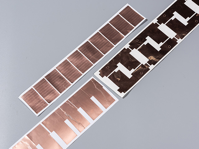
Many tight architectural spaces require a highly adaptable isolation solution. Electronic shielding tape fits perfectly into these demanding microscopic environments.
Profiles: You can source single-sided, double-sided, and ultra-thin transfer tapes. Some feature embedded conductive fabrics, while others use pure copper or aluminum foils.
Best for: They excel in extremely confined spaces. Engineers use them to replace bulky mechanical fasteners. They easily ground localized RF modules directly to a main chassis.
Rigid materials struggle with dynamic stress and thermal expansion. Elastomers offer a compliant, flexible alternative for modern housings.
Profiles: We see custom-dispensed liquid gaskets scaling down to 0.3mm widths. Manufacturers load these silicone matrices with microscopic silver, nickel, or graphite particles to create an electrical pathway.
Best for: Complex housing geometries require high mechanical flexibility. FIP silicones deliver extreme thermal stability across wide temperature ranges. They also support rapid automated CNC dispensing for global mass production lines.
Standard plastic and polycarbonate housings naturally let electromagnetic waves pass right through. You must metalize their inner surfaces to create an effective barrier.
Profiles: Assembly facilities spray specialized silver, nickel, or carbon-based liquid mixtures directly onto the raw plastic housings.
Best for: They provide broad, reliable system-level shielding. They coat highly complex, non-conductive enclosures effortlessly. Crucially, a sprayed coating does not consume any valuable internal Z-axis volume.
Selecting the right conductive material requires an analytical, data-driven approach. You must map specific electrical variables to distinct physical properties. Guesswork leads to failed compliance tests and redesigned housing molds.
Operating frequencies strictly dictate how electromagnetic waves interact with physical barriers. You must understand the underlying physics of your interference source.
Low Frequency (< 15 MHz): At low frequencies, you must focus entirely on magnetic permeability. Thick specialized alloys or steel panels work best here. They physically absorb the magnetic energy into their dense mass.
High Frequency (900 MHz+): At higher bandwidths, you must focus on surface conductivity. Above 900 MHz, the skin effect takes absolute control. Electromagnetic waves only travel along the extreme outer edge of the material. A barrier only needs to hit a ~0.05 mm thickness threshold to reflect the waves. This physical law makes thin foils and microscopic coatings highly viable for modern Wi-Fi and 5G applications.
Environmental stress will degrade chemically weak materials over time. You must anticipate the physical conditions of the end user.
First, consider compression realities. You must select elastomer gaskets based on precise compression rates. Typically, you need a strict 10% to 30% compression rate. Under-compressing the gasket causes immediate high-frequency shielding leaks. Over-compressing it destroys the polymer matrix and leads to permanent material deformation.
Second, you must aggressively mitigate galvanic corrosion. Dissimilar metals react destructively when exposed to high humidity. You can use a sealed conductive tape to isolate these conflicting metals. It creates an electrical bridge while simultaneously blocking moisture and oxygen from the vulnerable mating surfaces.
Modern engineering teams expect materials to perform more than one job simultaneously. You should actively evaluate components that combine EMI shielding with critical secondary physical properties. High-output processors generate immense, localized heat. Certain advanced conductive pads offer excellent thermal dissipation alongside their isolation capabilities. Others provide incredibly strong structural bonding. This multi-functional material approach heavily streamlines your overall internal design architecture.
Product Type | Primary Application Level | Frequency Focus | Key Secondary Function |
|---|---|---|---|
Metal Foils & Cans | Board-Level (PCB) | Low to Medium Frequency | Rigid structural protection |
Form-in-Place Gaskets | Enclosure-Level Sealing | High Frequency (900MHz+) | Environmental moisture sealing |
Conductive Coatings | System-Level Housing | High Frequency (Skin Effect) | Zero Z-axis space consumption |
Conductive Tapes | Targeted Grounding | Broadband Surface Grounding | Galvanic corrosion prevention |
A brilliant laboratory design fails instantly if you cannot manufacture it reliably. Scaling up to mass production introduces distinct, unpredictable assembly risks. You must evaluate production line constraints early in the drafting phase.
Form-in-Place (FIP) liquid gaskets require highly precise factory automation. You cannot ignore their rigid production realities. They require specific, unalterable curing times. Some fast-cure silicones need massive industrial heat ovens. Others rely on ambient atmospheric moisture over several hours. Your assembly line must accommodate these mandatory delays. Furthermore, you need specialized CNC dispensing equipment to maintain consistent bead profiles across thousands of units.
Sprayed coatings introduce a completely different set of physical challenges. You must implement strict fluid manufacturing controls. Conductive paints contain heavy, suspended metal particles. These solid particles settle rapidly at the bottom of the spray tank. You must continuously agitate and mix the paint during the entire application phase. If the metallic particles settle, the sprayed coating loses its continuous conductivity. This mistake creates invisible shielding blind spots on the final device housing.
Mechanical elasticity varies wildly in mass manufacturing. Rigid traditional shielding gaskets struggle to accommodate these standard elasticity tolerances. You risk over-compressing traditional stamped gaskets during the final screw assembly. This permanent damage warps the delicate mating surfaces. Instead, consider highly compliant options. You might combine beryllium copper shrapnel components with flexible metallic foils. This hybrid approach beautifully absorbs physical manufacturing shock. It handles housing variances effortlessly without ever breaking the crucial conductive seal.
Global electronics markets enforce strict, unforgiving electromagnetic compatibility rules. You must legally prove your device does not leak interference into the public spectrum.
Every single consumer device must meet established international regulatory standards before sale. In the United States, the FCC sets the strict legal baseline for allowable emissions. In Europe, you must achieve CE certification under specific radio equipment directives. Additionally, RoHS directives strictly limit the use of hazardous substances like lead. Your chosen shielding elements must comply entirely with all these intersecting environmental and electrical mandates.
Do not trust vague promotional marketing claims. You must interrogate vendor data sheets rigorously and scientifically.
Verify dB Attenuation Data: Always look for specific, charted attenuation values at your exact operating frequencies. Ensure the material provides sufficient decibel reduction at 2.4 GHz or 5.8 GHz, rather than relying on an unhelpful low-frequency average.
Check Surface Resistivity Metrics: Look closely for precise Ohms/square laboratory measurements. Lower surface resistivity directly and universally correlates to much better high-frequency wave reflection.
Always test selected materials inside physical device prototypes. We advise your engineering teams to request multiple sample batches early. You might test a specific flexible tape against a custom FIP silicone. Subject these physical prototypes to brutal real-world thermal cycling chambers. Use them to verify your specific internal gap calculations. The 1/20 wavelength rule remains your ultimate engineering guide. If thermal expansion creates a mechanical gap larger than 1/20 of your target operating wavelength, your shield will leak uncontrollably.
Choosing the correct material requires a highly deliberate engineering balancing act. You must align demanding frequency targets, microscopic Z-axis space limitations, and automated mass assembly capabilities. No single material magically solves every interference problem simultaneously. You must carefully tailor your component choice to the specific structural level of the frequency leak.
To move forward successfully, engineering and procurement teams should immediately map out their exact internal interference sources. Next, calculate the exact required dB attenuation for each isolated board zone. Finally, consult directly with a specialized material manufacturer. Request raw physical prototypes and conduct thorough thermal stress testing in your lab. A strictly data-driven approach ensures lasting device reliability and incredibly smooth global regulatory compliance.
A: Any mating surface gap must be smaller than 1/20th of the wavelength of the highest frequency being shielded to prevent RF leakage. If a physical seam exceeds this measurement, high-frequency electromagnetic waves will escape, instantly compromising your device's regulatory compliance and internal signal integrity.
A: Yes, for specific localized RF grounding and space-constrained areas, conductive tape reduces weight and assembly time significantly. It replaces bulky hardware in ultra-thin devices, though solid metal cans still remain the industry standard for covering heavy, high-output amplifier sections.
A: Typically 10% to 30%. Under-compression leads directly to dangerous EMI leaks because the seal fails to close gaps. Conversely, over-compression causes permanent material deformation, destroying the polymer matrix and leading to a complete loss of necessary mechanical elasticity.
A: No. At high frequencies (e.g., above 900 MHz), the skin effect dictates that electromagnetic waves only travel along the material's extreme outer surface. Therefore, increasing material thickness beyond approximately ~0.05mm offers absolutely negligible added shielding benefits while unnecessarily increasing weight.


